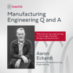
A Deep Dive into Cleanroom Packaging and Global Engineering with TransPak Expert
At TransPak, we’re proud to have a talented team of Subject Matter Experts whose creativity, knowledge, and dedication are the driving force behind the packaging solutions we deliver.
This summer, we’re highlighting the talented minds behind TransPak’s work through a special Q & A series. You’ll hear directly from our SMEs as they share their insights, challenges, and what drives their passion. It’s a behind-the-scenes look at the people who make TransPak a trusted partner for companies around the world.
Our first expert is Tom Hoekman, packaging engineering manager at TransPak. Based in the Netherlands, Tom brings decades of experience in cleanroom packaging design, engineering, and global manufacturing support.
We sat down with Tom to learn more about his path into engineering, his work with TransPak, and what makes cleanroom packaging for semiconductors a uniquely precise discipline.
Q: Tom, tell us about your background. What first sparked your interest in engineering?
Tom Hoekman:
I think my engineering career started when I was 5. I inherited two broken bicycles from my brothers, and I figured out how to combine parts from both to build one functioning bicycle. That’s when I started tightening bolts, greasing cogs, basically learning by doing.
Later, I studied industrial design engineering at university in the Netherlands. Since then, I’ve worked in packaging for over a decade.
Q: What does your role at TransPak involve?
Tom Hoekman:
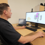
I lead two engineering teams. One focuses on new designs, working closely with key semiconductor industry customers, while the other supports what we call “build-to-print.” They take customer designs, manage sourcing, costing, and help translate those designs into scalable, global manufacturing solutions.
The team feeds this information back to the design team so they can start designing “local-for-local.” Many original designs are developed with European materials and suppliers. But when we build in the U.S., Asia, or elsewhere, those materials may not be available.
So we adapt designs, identify equivalent local materials, and ensure we still meet the same stringent cleanliness and performance standards for our customers. That global adaptability is one of TransPak’s unique strengths.
Another major focus of my role is cleanroom packaging. Semiconductor equipment is incredibly sensitive, so everything from the materials we use to how we assemble and clean each component must meet strict cleanliness and performance standards.
Q: Cleanroom packaging is a highly specialized discipline. What makes it so different from standard packaging?
Tom Hoekman:
The thing about cleanroom packaging is that the packaging needs to be as clean as the product, so our packaging has to comply with the same design rules. It’s very different from the typical wooden crates and soft packaging.
If you’re an engineer designing for cleanliness that can mean some extra steps along the way. We’re not just designing a box; we’re engineering an entire contamination control system. That means using materials like anodized aluminum, stainless steel, and high-performance plastics that have extremely low outgassing and particle release.
We layer multiple levels of protection: the cleanroom packaging itself, cleanroom-grade bags for molecular and particulate barriers, and then external crates to protect everything during transit. Every element of the system has to work together seamlessly.
Q: What are some of the other critical elements to consider when designing packaging for high-value semiconductor equipment?
Tom Hoekman:
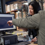
Cleanliness is obviously essential, but we also have to balance moisture control, electrostatic discharge (ESD) protection, and mechanical protection against shock and vibration. On top of that, there’s something people often overlook, and that’s human interaction.
When these tools arrive at a fab or a customer site, time is critical. We design packaging processes that allow engineers to unpack and install components as efficiently as possible. Downtime on a semiconductor manufacturing line is extremely costly, so our packaging essentially becomes part of the installation toolset.
Q: What do you think sets TransPak apart for customers in the semiconductor space?
Tom Hoekman:
It’s the global footprint. Very few companies in this space have the combination of global design, sourcing, and manufacturing expertise that TransPak offers. We’re able to share knowledge across regions, collaborate between teams, and translate complex designs into scalable solutions that work anywhere in the world.
Our customers come to us because we don’t just understand packaging, we understand their manufacturing processes, cleanroom standards, and business needs. We’re solving global engineering challenges, not just shipping problems.
Q: What do you enjoy doing outside of work?
Tom Hoekman:
I spend most of my free time with my family. We love being outdoors and going camping. This summer, we’re heading to the islands in the north of the Netherlands for a little vacation. It’s great to unplug and spend time outside.
Q: Finally — why did you choose to join TransPak?
Tom Hoekman:
For me, it was the international challenge. I’ve worked in this industry for years, but mostly in the Netherlands and Western Europe. TransPak gives me the opportunity to apply my expertise across the U.S., Asia, and beyond.
One day I’m talking to a team in America, the next day to a team in Korea. It’s constantly teaching me new things and allowing me to collaborate with colleagues across different cultures. That global perspective keeps the work exciting and meaningful.
Conclusion
At TransPak, cleanroom packaging isn’t just a product; it’s an engineered process. Experts like Tom bring together deep technical knowledge, global experience, and customer-focused design to deliver the highly specialized solutions today’s semiconductor industry demands.
To learn more about TransPak’s work in the semiconductor industry, visit our website.