Cleanroom Packaging Built for Today’s Semiconductor Supply Chain.
As semiconductor production surges across Southeast Asia, manufacturers are looking for partners who can match the precision, cleanliness, and reliability required for high-value components. TransPak Specialized Packaging (TSP) in Johor, Malaysia, was built specifically for that mission.
Opened in 2018 and now spanning more than 36,000 square feet, TSP serves as a regional center for cleanroom packaging, custom cases, foam fabrication, and reusable systems designed for semiconductor equipment and component manufacturers. More than 40 trained specialists work inside this purpose-built facility, combining engineering expertise, cleanroom-controlled environments, and advanced equipment to safeguard some of the most sensitive products in the global supply chain.
“As semiconductor manufacturing expands across Southeast Asia, customers need partners who are already embedded in the region and aligned with global standards,” said Aung Zeya, Regional Manager of Southeast Asia at TransPak. “With ISO-certified cleanrooms and contamination-controlled processes, TSP Johor gives customers localized speed while remaining fully connected to TransPak’s global engineering and logistics network.”
A Facility Engineered for Contamination-Sensitive Products
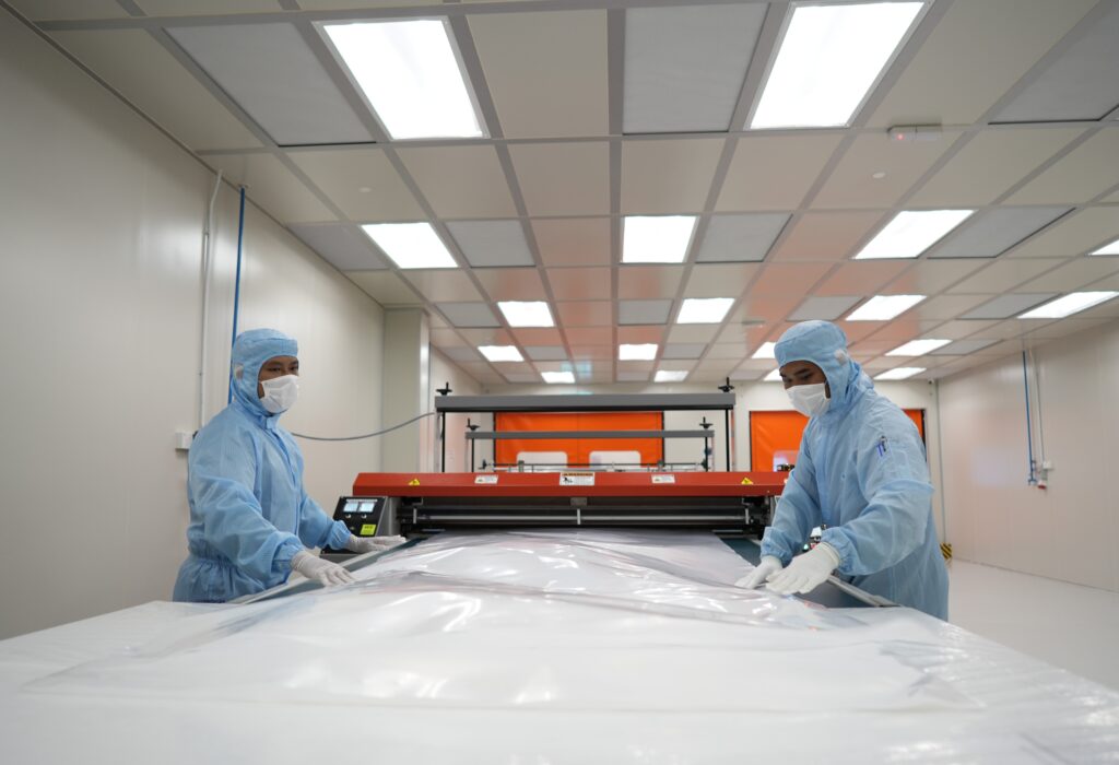
Semiconductor components, wafer-related materials, sensors, and precision assemblies all demand packaging that prevents even microscopic particulate exposure. To meet these requirements, TSP operates ISO-certified cleanrooms where temperature, humidity, airflow, and airborne particles are continuously regulated.
These controlled spaces allow TSP teams to package products that must remain free from surface interference. From gowning protocols to material flow, every step follows documented procedures and regulations aligned with semiconductor industry expectations.
Cleanroom Packaging for Ultra-Sensitive Components
At the core of TSP are its ISO 14644 Class 5 and Class 6 cleanrooms (equivalent to Class 100 and Class 1000). These rooms are monitored around the clock for particulate levels, environmental stability, and filtration performance. A dedicated darkroom supports products requiring exceptionally tight cleanliness thresholds.
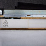
Inside these controlled environments, TSP produces a wide variety of flexible packaging materials, including:
- Flat, gusseted, and square-bottom bags
- Custom-cut bottom sheets
- Static-shielding, anti-static, and moisture-barrier LDPE materials
- Clean tube rolls for long or cylindrical components
- Perforated and non-perforated LDPE bubble rolls
For programs requiring highly repeatable packaging methods, TSP can recreate exact handling procedures and dimensions for consistency across production cycles—an essential requirement for many semiconductor customers.
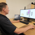
Engineering Complete Protection Systems
Beyond cleanroom packaging materials, TSP builds full protective ecosystems around delicate equipment and parts.
Custom Case Manufacturing
ATA cases, transit cases, and flight cases are built or refurbished to handle shock, vibration, and handling risks across global movement. These cases are used widely in fab environments, field service, and high-mix manufacturing support.
Advanced Foam Fabrication
With digital cutting equipment, band saws, and foam-splitting machines, TSP creates inserts tailored to complex geometries. Options include:
- Polyethylene foams (standard, laminated, anti-static, cross-linked)
- Polyurethane foams, including anti-static formulations
- Polypropylene corrugated sheets (standard, anti-static, conductive)
- Multi-wall corrugated board structures
These assemblies ensure that delicate components remain stable, cushioned, and aligned throughout transit.
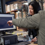
Quality Tools That Detect What Humans Cannot
To meet semiconductor inspection standards, TSP uses specialized measurement and verification tools, including:
- UV lamps to detect particulate contamination
- Dust particle counters for real-time environmental checks
- Static eliminators
- Thickness gauges and surface resistivity meters
- Precision measurement devices such as vernier calipers
Every component passes through protocols designed to support stringent semiconductor cleanliness requirements.
Strategic Location and Global Integration
Located in Johor’s growing semiconductor corridor, TSP serves manufacturers across Malaysia, Singapore, and the wider region with short lead times and rapid response. Its close integration with TransPak’s global network connects customers to engineering support, export compliance expertise, specialized crating, and logistics services, reducing handoffs and operational risk.
Supporting the Next Era of Semiconductor Manufacturing
As semiconductor technology advances, packaging partners must keep pace with rising cleanliness standards, tighter surface requirements, and faster production cycles. TSP Johor was built for exactly that: a controlled, repeatable, and dependable environment engineered for products that demand exceptional care.
By pairing contamination-controlled manufacturing with TransPak’s global capabilities, TSP continues to help semiconductor companies move critical components confidently and consistently across facilities, regions, and the world.
For cleanroom packaging built to meet semiconductor-grade standards, contact TransPak Specialized Packaging in Johor.